Power supply on tl494 with a midpoint. Scheme of a switching laboratory power supply on the TL494
THIS MATERIAL CONTAINS A LARGE NUMBER OF ANIMATED APPS!!!
For the Microsoft Internet Extlorer browser, you need to temporarily disable some features, namely:
- turn off integrated bars from Yandex, Google, etc.
- turn off the status bar (uncheck):
Turn off address bar:

Optionally, you can turn off the REGULAR BUTTONS, but the resulting screen area is already enough

Otherwise, no further adjustments are needed - the material is controlled using the buttons built into the material, and you can always return the removed panels to their place.
POWER CONVERSION
Before proceeding to describe the principle of operation of switching power supplies, one should recall some details from the general course of physics, namely what is electricity, what is a magnetic field and how they depend on each other.
We will not delve too deeply and we will also keep silent about the reasons for the appearance of electricity in various objects - for this you just need to stupidly retype 1/4 of the physics course, so we hope that the reader knows what electricity is not from the inscriptions on the signs "DO NOT GET IN - WILL KILL !". However, to begin with, let us recall what it happens to be, this is electricity itself, or rather voltage.

Well, now, purely theoretically, suppose that we have a conductor as a load, i.e. the most common piece of wire. What happens in it when current flows through it is clearly shown in the following figure:

If everything is clear with the conductor and the magnetic field around it, then we will fold the conductor not into a ring, but into several rings, so that our inductor will show itself more actively and see what happens next.

At this very place, it makes sense to drink tea and let the brain absorb what you just learned. If the brain is not tired, or this information is already known, then we look further

As power transistors in a switching power supply, bipolar transistors, field-effect (MOSFET) and IGBT are used. It is up to the device manufacturer to decide which power transistor to use, since both of them have their own advantages and disadvantages. However, it would be unfair not to notice that bipolar transistors are practically not used in powerful power supplies. MOSFET transistors are best used at conversion frequencies from 30 kHz to 100 kHz, but IGBTs "like frequencies lower - above 30 kHz it is better not to use them.
Bipolar transistors are good because they close pretty quickly, since the collector current depends on the base current, but in the open state they have a rather large resistance, which means that they will have a rather large voltage drop, which definitely leads to excessive heating of the transistor itself .
Field valves have very little active resistance in the open state, which does not cause a large release of heat. However, the more powerful the transistor, the greater its gate capacitance, and rather large currents are required to charge and discharge it. This dependence of the gate capacitance on the power of the transistor is due to the fact that the field-effect transistors used for power supplies are manufactured using MOSFET technology, the essence of which is the use of parallel connection of several field-effect transistors with an insulated gate and made on a single chip. And the more powerful the transistor, the more parallel transistors are used and the gate capacitances are summed up.
An attempt to find a compromise are transistors made using IGBT technology, since they are constituent elements. Rumor has it that they turned out purely by accident, when trying to repeat the MOSFET, but instead of field-effect transistors, they turned out not quite field and not quite bipolar. The gate of a low-power field-effect transistor built into the inside acts as a control electrode, which, with its source-drain, already controls the current of the bases of powerful bipolar transistors connected in parallel and made on the same chip of this transistor. Thus, a rather small gate capacitance and a not very large active resistance in the open state are obtained.
There are not so many basic circuits for switching on the power unit:
AUTOGENERATORY POWER SUPPLY. Use a positive connection, usually inductive. The simplicity of such power supplies imposes some limitations on them - such power supplies "like" a constant, unchanging load, since the load affects the feedback parameters. Such sources are both single-stroke and two-stroke.
PULSE POWER SUPPLY WITH FORCED EXCITATION. These power supplies are also divided into single-stroke and two-stroke. The former, although they are more loyal to the changing load, still do not maintain the necessary power reserve very steadily. And audio equipment has a rather large spread in consumption - in the pause mode, the amplifier consumes a few watts (the quiescent current of the final stage), and at the peaks of the audio signal, consumption can reach tens or even hundreds of watts.
Thus, the only, most acceptable option for a switching power supply for audio equipment is the use of push-pull circuits with forced excitation. Also, do not forget that during high-frequency conversion, it is necessary to pay more careful attention to filtering the secondary voltage, since the appearance of power interference in the audio range will nullify all efforts to manufacture a switching power supply for a power amplifier. For the same reason, the conversion frequency is moved further away from the audio range. The most popular conversion frequency used to be around 40 kHz, but the modern element base allows conversion at frequencies much higher - up to 100 kHz.
There are two basic types of these pulse sources - stabilized and not stabilized.
Stabilized power supplies use pulse-width modulation, the essence of which is to shape the output voltage by adjusting the duration of the voltage supplied to the primary winding, and the absence of pulses is compensated for by LC circuits connected at the secondary power output. A big plus of stabilized power supplies is the stability of the output voltage, which does not depend on the input voltage of the 220 V network or on the power consumption.
Non-stabilized ones simply control the power part with a constant frequency and pulse duration, and differ from a conventional transformer only in dimensions and much smaller capacitances of the secondary power capacitors. The output voltage directly depends on the 220 V network, and has a slight dependence on the power consumption (at idle, the voltage is slightly higher than the calculated one).
The most popular schemes for the power part of switching power supplies are:
Midpoint(PUSH-PULL). They are usually used in low-voltage power supplies, since it has some features in the requirements for the element base. The power range is quite large.
Half bridge. The most popular circuit in network switching power supplies. Power range up to 3000 W. A further increase in power is possible, but already at a cost it reaches the level of the bridge version, therefore it is somewhat uneconomical.
Bridges. This circuit is not economical at low powers, since it contains twice the number of power switches. Therefore, it is most often used at powers from 2000 watts. The maximum power is in the range of 10,000 watts. This circuitry is the main one in the manufacture of welding machines.
Let's take a closer look at who is who and how it works.
WITH MIDDLE POINT

As it was shown, this circuitry of the power section is not recommended to be used to create network power supplies, but NOT RECOMMENDED does not mean IMPOSSIBLE. You just need to be more careful in choosing the element base and manufacturing the power transformer, as well as taking into account rather high voltages when laying the printed circuit board.
This power stage received the maximum popularity in automotive audio equipment, as well as in uninterruptible power supplies. However, in this field, this circuitry suffers some inconvenience, namely the limitation of maximum power. And the point is not in the element base - today MOSFET transistors with instantaneous drain-source current values of 50-100 A are not at all scarce. The point is in the overall power of the transformer itself, or rather in the primary winding.
The problem is ... However, for greater persuasiveness, we will use the program for calculating winding data of high-frequency transformers.
Let's take 5 rings of size K45x28x8 with a permeability M2000HM1-A, set the conversion frequency to 54 kHz and the primary winding to 24 V (two half-windings of 12 V each). As a result, we get that the power of this core can develop 658 watts, but the primary winding should contain 5 turns , i.e. 2.5 turns per half winding. As it is not naturally enough ... However, it is worth raising the conversion frequency to 88 kHz, as it turns out only 2 (!) turns per half-winding, although the power looks very tempting - 1000 watts.
It seems that you can put up with such results and distribute 2 turns evenly over the entire ring, too, if you try hard, you can, but the quality of the ferrite leaves much to be desired, and the M2000HM1-A at frequencies above 60 kHz already heats up quite strongly by itself, well, at 90 kHz it already needs to be blown.
So whatever one may say, but it turns out a vicious circle - by increasing the dimensions to obtain more power, we reduce the number of turns of the primary winding too much, by increasing the frequency, we again reduce the number of turns of the primary winding, but in addition we get excess heat.
It is for this reason that dual converters are used to obtain powers above 600 W - one control module outputs control pulses to two identical power modules containing two power transformers. The output voltages of both transformers are summed. It is in this way that the power supply of factory-made heavy-duty car amplifiers is organized and about 500..700 W and no more are removed from one power module. There are several ways to sum up:
- summation of alternating voltage. The current in the primary windings of the transformers is supplied synchronously, therefore the output voltages are synchronous and can be connected in series. It is not recommended to connect the secondary windings in parallel from two transformers - a small difference in winding or quality of the ferrite leads to large losses and a decrease in reliability.
- summation after rectifiers, i.e. constant voltage. The best option - one power module produces a positive voltage for the power amplifier, and the second - a negative one.
- power generation for amplifiers with two-level power supply by adding two identical bipolar voltages.
HALF-BRIDGE

The half-bridge circuit has quite a few advantages - it is simple, therefore reliable, easy to repeat, does not contain scarce parts, and can be performed on both bipolar and field-effect transistors. The IGBT transistors in it also work fine. However, she has a weak spot. These are bypass capacitors. The fact is that at high powers a rather large current flows through them and the quality of the finished switching power supply directly depends on the quality of this particular component.
And the problem is that the capacitors are constantly recharged, therefore they must have a minimum OUTPUT-COVERING resistance, since with a large resistance, quite a lot of heat will be released in this area and in the end the output will simply burn out. Therefore, film capacitors must be used as pass-through capacitors, and the capacitance of one capacitor can reach a capacitance of 4.7 μF in the extreme case, if one capacitor is used - a circuit with one capacitor is also quite often used, according to the principle of the UMZCH output stage with unipolar power supply. If two 4.7 uF capacitors are used (their connection point is connected to the transformer winding, and the free terminals are connected to the positive and negative power buses), then this equipment is quite suitable for powering power amplifiers - the total capacitance for the alternating voltage of the conversion adds up and, as a result, it turns out equal to 4.7 uF + 4.7 uF = 9.4 uF. However, this option is not designed for long-term continuous use with maximum load - it is necessary to divide the total capacitance into several capacitors.
If it is necessary to obtain large capacities (low conversion frequency), it is better to use several capacitors of a smaller capacity (for example, 5 pieces of 1 uF connected in parallel). However, a large number of capacitors connected in parallel rather greatly increases the dimensions of the device, and the total cost of the entire garland of capacitors is not small. Therefore, if you need to get more power, it makes sense to use a bridge circuit.
For a half-bridge version, powers above 3000 W are not desirable - boards with feed-through capacitors will be painfully bulky. The use of electrolytic capacitors as feed-through capacitors makes sense, but only at powers up to 1000 W, since electrolytes are not effective at high frequencies and start to warm up. Paper capacitors as feedthroughs have shown themselves very well, but here are their dimensions ...
For greater clarity, we give a table of the dependence of the reactance of the capacitor on frequency and capacitance (Ohm):
| Capacitor capacity |
conversion frequency |
|||||||
Just in case, we remind you that when using two capacitors (one for plus, the second for minus), the final capacitance will be equal to the sum of the capacitances of these capacitors. The resulting resistance does not generate heat, since it is reactive, but it can affect the efficiency of the power supply at maximum loads - the output voltage will begin to decrease, despite the fact that the overall power of the power transformer is quite sufficient.
BRIDGE

The bridge circuit is suitable for any power, but is most effective at high powers (for mains power supplies, these are powers from 2000 W). The circuit contains two pairs of power transistors controlled synchronously, but the need for galvanic isolation of the emitters of the upper pair introduces some inconvenience. However, this problem is completely solvable when using control transformers or specialized microcircuits, for example, for field-effect transistors, you can use IR2110 - a specialized development of International Rectifier.
However, the power section has no meaning if it is not controlled by the control module.
There are quite a lot of specialized microcircuits capable of controlling the power part of switching power supplies, however, the most successful development in this area is TL494, which appeared in the last century, however, has not lost its relevance, since it contains ALL the necessary nodes for controlling the power part of switching power supplies . The popularity of this microcircuit is primarily evidenced by its release by several large manufacturers of electronic components at once.
Consider the principle of operation of this microcircuit, which with full responsibility can be called a controller, since it has ALL the necessary nodes.


PART II
What is the actual PWM method of voltage regulation?
The method is based on the same inertia of inductance, i.e. its not the ability to instantly pass the current. Therefore, by adjusting the duration of the pulses, you can change the final constant voltage. Moreover, for switching power supplies, it is better to do this in primary circuits and thus save money on creating a power source, since this source will play two roles at once:
- voltage conversion;
- stabilization of the output voltage.
Moreover, much less heat will be generated in this case compared to a linear stabilizer installed at the output of a non-stabilized switching power supply.
For more clarity, see the figure below:
![]()
The figure shows the equivalent circuit of a switching regulator in which the generator of rectangular pulses V1 acts as a power switch, and R1 as a load. As can be seen from the figure, with a fixed output pulse amplitude of 50 V, by changing the pulse duration, it is possible to change the voltage supplied to the load over a wide range, and with very small thermal losses, depending only on the parameters of the power switch used.
We figured out the principles of operation of the power unit, as well as management. It remains to connect both nodes and get a ready-made switching power supply.
The load capacity of the TL494 controller is not very large, although it is enough to control one pair of power transistors of the IRFZ44 type. However, for more powerful transistors, current amplifiers are already needed that can develop the required current at the control electrodes of power transistors. Since we are trying to reduce the size of the power supply and move away from the audio range, MOSFETs will be the best use as power transistors.

Variants of structures in the manufacture of MOSFETs.
On the one hand, large currents are not needed to control a field-effect transistor - they are opened by voltage. However, there is a fly in the ointment in this barrel of honey, in this case, which consists in the fact that although the gate has a huge active resistance that does not consume current to drive the transistor, the gate has a capacitance. And for its charge and discharge, large currents are just needed, since at high conversion frequencies, the reactance is already reduced to limits that cannot be ignored. And the greater the power of the power MOSFET transistor, the greater the capacitance of its gate.
For example, take the IRF740 (400V, 10A) which has a gate capacitance of 1400pF and the IRFP460 (500V, 20A) which has a gate capacitance of 4200pF. Since both the first and the second gate voltage should not exceed ± 20 V, then we take a voltage of 15 V as control pulses and see in the simulator what happens at a generator frequency of 100 kHz on resistors R1 and R2, which are connected in series with capacitors at 1400 pF and 4200 pF.

Test stand.
When a current flows through an active load, a voltage drop forms on it; by this value, one can judge the instantaneous values of the flowing current.

Drop across resistor R1.
As can be seen from the figure, immediately upon the appearance of a control pulse, approximately 10.7 V drops across the resistor R1. With a resistance of 10 ohms, this means that the instantaneous current value reaches 1, A (!). As soon as the pulse ends on the resistor R1, 10.7 V also drops, therefore, in order to discharge the capacitor C1, a current of about 1 A is required ..
To charge and discharge a 4200 pF capacitance through a 10 ohm resistor, 1.3 A is required, since 13.4 V drops across the 10 ohm resistor.

The conclusion suggests itself - for charging and discharging the capacitances of the gates, it is necessary that the helmet operating on the gates of power transistors withstand fairly large currents, despite the fact that the total consumption is quite small.
To limit the instantaneous current values in the gates of field-effect transistors, current-limiting resistors from 33 to 100 ohms are usually used. An excessive decrease in these resistors increases the instantaneous value of the flowing currents, and an increase increases the duration of the power transistor in linear mode, which leads to unreasonable heating of the latter.
Quite often, a chain is used consisting of a resistor and a diode connected in parallel. This trick is used primarily to unload the control stage during charging and accelerate the discharge of the gate capacitance.

A fragment of a single-cycle converter.
Thus, not an instantaneous appearance of current in the winding of a power transformer is achieved, but somewhat linear. Although this increases the temperature of the power stage, it quite noticeably reduces the self-oscillation spikes that inevitably appear when a square-wave voltage is applied to the transformer winding.

Self-induction in the operation of a single-cycle converter
(red line - voltage on the transformer winding, blue - supply voltage, green - control pulses).
So we figured out the theoretical part and we can draw some conclusions:
To create a switching power supply, a transformer is needed, the core of which is made of ferrite;
To stabilize the output voltage of a switching power supply, a PWM method is required, which the TL494 controller quite successfully copes with;
The power part with a midpoint is most convenient for low-voltage switching power supplies;
The power part of half-bridge circuitry is convenient for small and medium powers, and its parameters and reliability largely depend on the number and quality of feed-through capacitors;
The power part of the bridge type is more beneficial for large powers;
When used in the power section of the MOSFET, do not forget about the capacitance of the gates and calculate the control elements with power transistors, corrected for this capacitance;
Since we figured out the individual nodes, we move on to the final version of the switching power supply. Since the algorithm and circuitry of all half-bridge sources are almost the same, to clarify which element is needed for what, we will analyze the most popular one, with a power of 400 W, with two bipolar output voltages.

It remains to note a few nuances:
Resistors R23, R25, R33, R34 serve to create an RC filter, which is highly desirable when using electrolytic capacitors at the output of switching sources. Ideally, of course, it is better to use LC filters, but since the "consumers" are not very powerful, you can completely get by with an RC filter. The resistance of these resistors can be used from 15 to 47 ohms. R23 is better with a power of 1 W, the rest at 0.5 W is enough.
C25 and R28 - a snubber that reduces self-induction emissions in the power transformer winding. They are most effective at capacitances above 1000 pF, but in this case too much heat is generated on the resistor. Necessary in the case when there are no chokes after the rectifier diodes of the secondary power supply (the vast majority of factory equipment). If chokes are used, the effectiveness of snubbers is not as noticeable. Therefore, we rarely install them and the power sources do not work worse from this.
If some values of the elements differ on the board and the circuit diagram, these values are not critical - you can use both.
If there are elements on the board that are not on the circuit diagram (usually these are power capacitors), then you can not install them, although it will be better with them. If you decide to install, then not electrolytic capacitors can be used at 0.1 ... 0.47 μF, but electrolytic ones of the same capacity as those that are obtained with them connected in parallel.
On the board OPTION 2 Near the radiators there is a rectangular part that is drilled around the perimeter and power supply control buttons (on-off) are installed on it. The need for this hole is due to the fact that the 80 mm fan does not fit in height in order to fix it to the radiator. Therefore, the fan is mounted below the PCB base.

INSTRUCTIONS FOR SELF-ASSEMBLY
STABILIZED SWITCH POWER SUPPLY
To begin with, you should carefully read the circuit diagram, however, this should always be done before proceeding with the assembly. This voltage converter operates on a half-bridge circuit. What is the difference from the rest is described in detail.

The circuit diagram is packaged with WinRAR of the old version and executed on a WORD-2000 page, so there should be no problems with printing this page. Here we will consider its fragments, since we want to keep the scheme highly readable, but it does not fit entirely on the screen of the monitor. Just in case, you can use this drawing to represent the picture as a whole, but it's better to print ...
Figure 1 - filter and mains voltage rectifier. The filter is intended primarily to exclude the penetration of impulse noise from the converter into the network. Made on L-C basis. A ferrite core of any shape is used as an inductance (rod is better not needed - a large background from them) with a wound single winding. The dimensions of the core depend on the power of the power source, since the more powerful the source, the more interference it will create and the better the filter is needed.

Picture 1.
The approximate dimensions of the cores, depending on the power of the power source, are summarized in Table 1. The winding is wound until the core is filled, the diameter (s) of the wire should be selected based on 4-5 A/mm2.
| Table 1 | ||||
|
POWER SUPPLY POWER |
RING CORE |
W-SHAPED CORE |
||
|
Diameter from 22 to 30 with a thickness of 6-8 mm |
Width from 24 to 30 with a thickness of 6-8 mm |
|||
|
Diameter from 32 to 40 with a thickness of 8-10 mm |
Width from 30 to 40 with a thickness of 8-10 mm |
|||
|
Diameter from 40 to 45 with a thickness of 8-10 mm |
Width from 40 to 45 with a thickness of 8-10 mm |
|||
|
Diameter from 40 to 45 with a thickness of 10-12 mm |
Width from 40 to 45 with a thickness of 10-12 mm |
|||
|
Diameter from 40 to 45 with a thickness of 12-16 mm |
Width from 40 to 45 with a thickness of 12-16 mm |
|||
|
Diameter from 40 to 45 with a thickness of 16-20 mm |
Width from 40 to 45 with a thickness of 16-20 mm |
|||
Here it should be explained a little why the diameter (s) and what is 4-5 A / mm sq.
This category of power supplies belongs to the high-frequency. Now let's remember the course of physics, namely the place that says that at high frequencies the current does not flow over the entire cross section of the conductor, but over its surface. And the higher the frequency, the greater part of the conductor section remains unused. For this reason, in pulsed high-frequency devices, the windings are made using bundles, i.e. several thinner conductors are taken and added together. Then the resulting bundle is twisted slightly along the axis so that the individual conductors do not stick out in different directions during winding, and the windings are wound with this bundle.
4-5 A / mm kv means that the tension in the conductor can reach from four to five amperes per square millimeter. This parameter is responsible for heating the conductor due to the voltage drop in it, because the conductor has, although not large, but still resistance. In pulse technology, winding products (chokes, transformers) have relatively small dimensions, therefore they will be well cooled, so the tension can be used exactly 4-5 A / mm sq. But for traditional transformers made on iron, this parameter should not exceed 2.5-3 A / mm sq. How many wires and what section will help to calculate the plate of diameters. In addition, the plate will tell you what power can be obtained by using one or another number of wires of the available wire, if you use it as the primary winding of a power transformer. Open plate.
The capacitance of the capacitor C4 must be at least 0.1 uF, if it is used at all. Voltage 400-630 V. Formulation if it is used at all it is not used in vain - the main filter is the inductor L1, and its inductance turned out to be quite large and the probability of penetration of high-frequency interference is reduced to almost zero values.
Diode bridge VD is used to rectify the alternating mains voltage. As a diode bridge, an RS-type assembly (end terminals) is used. For a power of 400 W, you can use RS607, RS807, RS1007 (at 700 V, 6, 8 and 10 A, respectively), since the installation dimensions of these diode bridges are the same.
Capacitors C7, C8, C11 and C12 are necessary to reduce the impulse noise created by the diodes when the AC voltage approaches zero. The capacitance of these capacitors is from 10 nF to 47 nF, the voltage is not lower than 630 V. However, after several measurements, it was found that L1 copes well with these interferences, and capacitor C17 is enough to eliminate the influence on the primary circuits. In addition, the capacitances of capacitors C26 and C27 also contribute - for the primary voltage, they are two capacitors connected in series. Since their ratings are equal, the final capacitance is divided by 2 and this capacitance not only serves to operate the power transformer, but also suppresses impulse noise on the primary power supply. Based on this, we abandoned the use of C7, C8, C11 and C12, but if someone really wants to install them, then there is enough space on the board, from the side of the tracks.
The next fragment of the circuit is the current limiters on R8 and R11 (Figure 2). These resistors are necessary to reduce the charging current of electrolytic capacitors C15 and C16. This measure is necessary because a very large current is required at the moment of switching on. Neither the fuse nor the VD diode bridge are capable of, even for a short time, withstanding such a powerful current surge, although the inductance L1 limits the maximum value of the flowing current, in this case this is not enough. Therefore, current-limiting resistors are used. The power of 2 W resistors was chosen not so much because of the heat generated, but because of the rather wide resistive layer that can withstand a current of 5-10 A for a short time. For power supplies up to 600 W, you can use resistors with power and 1 W, or use one resistor power of 2 W, it is only necessary to comply with the condition - the total resistance of this circuit should not be less than 150 ohms and should not be more than 480 ohms. If the resistance is too low, the chance of destruction of the resistive layer increases, if it is too high, the charge time for C15, C16 increases and the voltage on them does not have time to approach the maximum value when relay K1 operates and the contacts of this relay will have to switch too much current. If wire-wound resistors are used instead of MLT resistors, then the total resistance can be reduced to 47 ... 68 ohms.
The capacitance of capacitors C15 and C16 is also selected depending on the power of the source. You can calculate the required capacity using a simple formula: ONE WATT OF OUTPUT POWER REQUIRES 1 µF OF PRIMARY POWER FILTER CAPACITORS. If you have doubts about your mathematical abilities, you can use the plate, in which you simply put the power of the power source that you are going to make and see how many and what kind of capacitors you need. Please note that the board is designed for the installation of network electrolytic capacitors with a diameter of 30 mm.
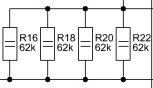
Figure 3
Figure 3 shows the quenching resistors, the main purpose of which is to form the starting voltage. The power is not lower than 2 W, they are installed on the board in pairs, one above the other. Resistance from 43 kOhm to 75 kOhm. It is VERY desirable that ALL resistors be of the same rating - in this case, the heat is distributed evenly. For small powers, a small relay with low consumption is used, so 2 or three quenching resistors can be dispensed with. On the board are installed on top of each other.

Figure 4
Figure 4 - power supply regulator of the control module - in any case, an intergarl regulator for + 15V. Requires a radiator. Size ... Usually, a radiator from the penultimate cascade of domestic amplifiers is enough. You can ask for something in TV workshops - TV boards usually have 2-3 suitable radiators. The second one is just used to cool the VT4 transistor, which controls the fan speed (Figure 5 and 6). Capacitors C1 and C3 can also be used at 470 uF at 50 V, but this replacement is only suitable for power supplies using a certain type of relay, in which the coil resistance is quite large. On more powerful sources, a more powerful relay is used and a decrease in the capacitance of C1 and C3 is highly undesirable.

Figure 5 
Figure 6
Transistor VT4 - IRF640. Can be replaced with IRF510, IRF520, IRF530, IRF610, IRF620, IRF630, IRF720, IRF730, IRF740, etc. AND.
Transistor VT1 - almost any direct transistor with a maximum current of more than 1 A, preferably with a small saturation voltage. Transistors in the TO-126 and TO-220 cases become equally good, so you can pick up a lot of replacements. If you screw a small radiator, then even KT816 is quite suitable (Figure 7).

Figure 7
Relay K1 - TRA2 D-12VDC-S-Z or TRA3 L-12VDC-S-2Z. In fact, it is the most ordinary relay with a 12 V winding and a contact group capable of switching 5 A or more. You can use the relays used in some TVs to turn on the demagnetization loop, just keep in mind that the contact group in such relays has a different pinout, and even if it gets on the board without any problems, you should check which pins close when voltage is applied to the coil. TRA2 differs from TRA3 in that TRA2 has one contact group capable of switching current up to 16 A, and TRA3 has 2 contact groups of 5A each.
By the way, the printed circuit board is offered in two versions, namely with the use of a relay and without it. The version without a relay does not use the primary voltage soft start system, therefore this option is suitable for a power supply with a power of not more than 400 W, since it is highly not recommended to switch on a "direct" capacitance of more than 470 uF without current limiting. In addition, a bridge with a maximum current of 10 A MUST be used as a VD diode bridge, i.e. RS1007. Well, the role of the relay in the version without soft start is performed by the LED. The standby function is saved.
Buttons SA2 and SA3 (it is assumed that SA1 is a power switch) - buttons of any type without fixation, for which you can make a separate printed circuit board, or you can grind it in another convenient way. It must be remembered that button contacts are galvanically connected to the 220 V network, therefore, it is necessary to exclude the possibility of their contact during the operation of the power source.
There are quite a few analogues of the TL494 controller, you can use any, just keep in mind that different manufacturers may have some differences in parameters. For example, when replacing one manufacturer with another, the conversion frequency may change, but not much, but the output voltage may change up to 15%.
IR2110, in principle, is not a scarce driver, and it does not have many analogues - IR2113, but IR2113 has more package options, so be careful - you need a DIP-14 package.
When mounting the board, instead of microcircuits, it is better to use connectors for microcircuits (sockets), ideally - collet, but ordinary ones can also be used. This measure will avoid some misunderstandings, since there are quite a lot of marriages among both TL494 (no output pulses, although the clock generator works), and among IR2110 (no control pulses to the upper transistor), so the warranty conditions should be agreed with the seller of microcircuits.

Figure 8
Figure 8 shows the power section. It is better to use fast diodes VD4 ... VD5, for example SF16, but in the absence of such, HER108 is also quite suitable. C20 and C21 - a total capacitance of at least 1 uF, so you can use 2 capacitors of 0.47 uF. The voltage is at least 50 V, ideally - a film capacitor of 1 μF 63 V (in the event of a breakdown of power transistors, the film remains intact, and the multilayer ceramic dies). For power supplies up to 600 W, the resistance of resistors R24 and R25 can be from 22 to 47 ohms, since the gate capacitances of power transistors are not very large.
Power transistors can be any of those given in table 2 (case TO-220 or TO-220R).
| table 2 | ||||||
|
Name |
gate capacitance, |
Max voltage, |
Max current, |
thermal power, |
Resistance, |
|
|
|
||||||
| If the thermal power does not exceed 40 W, then the transistor housing is completely plastic and a larger heat sink is required in order not to bring the crystal temperature to a critical value. Gate voltage for all no more than ±20 V |
||||||

Thyristors VS1 and VS, in principle, the brand does not matter, the main thing is that the maximum current must be at least 0.5 A and the case must be TO-92. We use either MCR100-8 or MCR22-8.
Diodes for low-current power supply (Figure 9) are desirable to choose with a short recovery time. Diodes of the HER series, such as HER108, are quite suitable, but others can also be used, such as SF16, MUR120, UF4007. Resistors R33 and R34 for 0.5 W, resistance from 15 to 47 ohms, with R33 \u003d R34. The service winding operating on VD9-VD10 must be rated for 20 V stabilized voltage. In the winding calculation table, it is marked in red.

Figure 9
Power rectifier diodes can be used both in the TO-220 package and in the TO-247 package. In both versions of the printed circuit board, it is assumed that the diodes will be installed one above the other and connected to the board with conductors (Figure 10). Of course, when installing diodes, thermal paste and insulating gaskets (mica) should be used.

Figure 10
As rectifier diodes, it is desirable to use diodes with a short recovery time, since the heating of the diodes at idle depends on this (the internal capacitance of the diodes affects and they simply heat up on their own, even without load). The list of options is summarized in table 3
| Table 3 | |||
|
Name |
Max voltage, |
maximum current, |
recovery time, |
The current transformer performs two roles - it is used precisely as a current transformer and as an inductance connected in series with the primary winding of the power transformer, which allows to slightly reduce the rate of current appearance in the primary winding, which leads to a decrease in self-induction emissions (Figure 11).

Figure 11
There are no strict formulas for calculating this transformer, but it is strongly recommended to observe some restrictions:
| FOR POWERS FROM 200 TO 500 W - RING WITH DIAMETER 12...18 MM FOR POWER FROM 400 TO 800 W - RING WITH DIAMETER 18...26 MM FOR POWER FROM 800 TO 1800 W - RING WITH DIAMETER 22...32 MM FOR POWER FROM 1500 TO 3000 W - RING WITH DIAMETER 32...48 MM |
FERRITE RINGS, PERMEABILITY 2000, THICKNESS 6...12 MM |
NUMBER OF TURNS OF THE PRIMARY WINDING:
3 TURNS FOR BAD COOLING CONDITIONS AND 5 TURNS IF THE FAN BLOWS DIRECTLY ON THE BOARD
NUMBER OF TURNS OF THE SECONDARY WINDING:
12...14 FOR PRIMARY OF 3 TURNS AND 20...22 FOR PRIMARY OF 5 TURNS
IT IS MUCH MORE CONVENIENT TO WIND THE TRANSFORMER SECTIONALLY - THE PRIMARY WINDING DOES NOT LOCK WITH THE SECONDARY. IN THIS CASE, IT IS NO WORK TO REWIND-REWIND THE COIL TO THE PRIMARY WINDING. IN THE FINAL WHEN THE LOAD IS 60% FROM THE MAXIMUM ON THE UPPER OUTPUT R27 SHOULD BE ABOUT 12 ... 15 V
The primary winding of the transformer is wound in the same way as the primary winding of the power transformer TV2, secondary with a double wire with a diameter of 0.15 ... 0.3 mm.
For the manufacture of a power transformer of a pulsed power supply, you should use the program for calculating pulse transformers. The design of the core is of no fundamental importance - it can be both toroidal and W-shaped. Printed circuit boards allow you to use both without problems. If the overall capacity of the W-shaped medium is not enough, it can also be folded into a package, like rings (Figure 12).

Figure 12
You can get hold of W-shaped ferrites in TV workshops - not often, but the power transformers in TVs fail. The easiest way to find power supplies from domestic TVs is the 3rd ... 5th. Do not forget that if a transformer of two or three mediums is required, then ALL mediums must be of the same brand, i.e. for disassembly, it is necessary to use transformers of the same type.
If the power transformer is made of rings 2000, then table 4 can be used.
|
IMPLEMENTATION |
REAL |
PARAMETER |
CONVERSION FREQUENCY |
||||||
|
POSSIBLE MORE |
OPTIMAL |
STRONG HEAT |
|||||||
|
1 RING |
OVERALL POWER |
||||||||
| TURNS ON THE FIRST WINDING | |||||||||
|
2 RINGS |
OVERALL POWER |
||||||||
| TURNS ON THE FIRST WINDING | |||||||||
|
1 RING |
OVERALL POWER |
||||||||
| TURNS ON THE FIRST WINDING | |||||||||
|
2 RINGS |
OVERALL POWER |
||||||||
| TURNS ON THE FIRST WINDING | |||||||||
|
3 RINGS |
OVERALL POWER |
|
|
|
|||||
| TURNS ON THE FIRST WINDING |
|
|
|
||||||
|
4 RINGS A |
OVERALL POWER |
|
|
|
|
|
|||
| TURNS ON THE FIRST WINDING |
|
|
|
|
|
||||
| THE NUMBER OF WINDINGS OF THE SECONDARY WINDING IS CALCULATED THROUGH THE PROPORTION, CONSIDERING THE VOLTAGE ON THE PRIMARY WINDING IS 155 V OR USING THE TABLE ( CHANGE ONLY YELLOW CELLS) | |||||||||
Please note that voltage stabilization is carried out using PWM, therefore the output rated voltage of the secondary windings must be at least 30% more than you need. The optimal parameters are obtained when the calculated voltage is 50 ... 60% more than it is necessary to stabilize. For example, you need a source with an output voltage of 50 V, therefore, the secondary winding of a power transformer must be designed for an output voltage of 75 ... 80 V. In the table for calculating the secondary winding, this coefficient is taken into account.
The dependence of the conversion frequency on the ratings of C5 and R5 is shown in the graph:

It is not recommended to use a fairly large resistance R5 - too large a magnetic field is not far at all and pickups are possible. Therefore, we will focus on the "average" R5 rating of 10 kOhm. With such a resistance of the frequency-setting resistor, the following conversion frequencies are obtained:
|
Parameters obtained from this manufacturer |
conversion frequency |
||
|
|
|||

(!) Here a few words should be said about the winding of the transformer. Quite often, disturbances come, they say, when self-made, the source either does not give the necessary power, or the power transistors get very hot even without load.
Frankly speaking, we also encountered such a problem using 2000 rings, but it was easier for us - the presence of measuring equipment made it possible to find out what the reason for such incidents was, and it turned out to be quite expected - the magnetic permeability of the ferrite does not correspond to the marking. In other words, on "weak" transformers, the primary winding had to be unwound, on the contrary, on "heating power transistors" - to wind up.
A little later, we abandoned the use of rings, however, the ferrite that we use was not masked at all, so we took drastic measures. A transformer with the estimated number of turns of the primary winding is connected to the assembled and debugged board and the conversion frequency is changed by the trimming resistor installed on the board (instead of R5, a 22 kOhm trimmer is installed). At the moment of switching on, the conversion frequency is set within 110 kHz and starts to decrease by rotating the tuning resistor engine. Thus, the frequency at which the core begins to saturate is found out, i.e. when the power transistors start to warm up without load. If the frequency drops below 60 kHz, then the primary winding is unwound; if the temperature starts to rise by 80 kHz, then the primary winding is rewound. Thus, the number of turns for this particular core is determined, and only after that the secondary winding is wound using the plate proposed above, and the number of turns of the primary for one or another medium is indicated on the packages.
If the quality of your core is in doubt, then it is better to make a board, check it for operability, and only after that make a power transformer using the method described above.
Throttle group stabilization. In some places, even the judgment flashed that he couldn’t work in any way, since a constant voltage flows through him. On the one hand, such judgments are correct - the voltage is really of the same polarity, which means it can be recognized as constant. However, the author of such a judgment did not take into account the fact that the voltage, although constant, is pulsating, and during operation, not one process (current flow) occurs in this node, but many, since the inductor contains not one winding, but at least two (if output voltage needs bipolar) or 4 windings if two bipolar voltages are needed (Figure 13).

It is possible to make a choke both on the ring and on the W-shaped ferrite. Dimensions of course depend on the power. For powers up to 400-500 W, a medium is enough from a surge protector for powering TVs with a diagonal of 54 cm and above (Figure 14). Core design is not critical
Figure 14
It is wound in the same way as a power transformer - from several thin conductors twisted into a bundle or glued into a tape at the rate of 4-5 A / mm sq. Theoretically - the more turns - the better, so the winding is laid before the window is filled, and immediately in 2 (if you need a bipolar source) or 4 wires (if you need a source with two bipolar voltages.
After smoothing capacitors are output chokes. There are no special requirements for them, dimensions ... The boards are designed for the installation of cores from TV mains power filters. Wind up until the window is filled, cross section at the rate of 4-5 A / mm sq (Figure 15).


Figure 15
The tape was mentioned above as a winding. Here it is necessary to stop a little more in detail.
What's better? Tie or tape? Both of these methods have their advantages and disadvantages. Making a bundle is the easiest way - stretched the required number of wires, and then twisted them into a bundle using a drill. However, this method increases the total length of the conductors due to internal torsion, and also does not allow achieving the identity of the magnetic field in all conductors of the bundle, and this, although not large, is still heat loss.
The production of the tape is more labor-intensive and a little more expensive, since the required number of conductors is stretched and then, with the help of polyurethane glue (TOP-TOP, SPECIALIST, MOMENT-CRYSTAL) is glued into a tape. The glue is applied to the wire in small portions - 15 ... 20 cm long of the conductor, and then, holding the bundle between the fingers, they rub it, as it were, making sure that the wires fit into the tape, similar to tape bundles used to connect disk media to the motherboard of IBM computers. After the glue has stuck, a new portion is applied to 15 ... 20 cm of the length of the wires and smoothed again with your fingers until a tape is obtained. And so along the entire length of the conductor (Figure 16).

Figure 16
After the glue has completely dried, the tape is wound on the core, and the winding with a large number of turns (as a rule, with a smaller cross section) is wound first, and more high-current windings are already on top. After winding the first layer, it is necessary to “lay” the tape inside the ring using a cone-shaped peg cut from wood. The maximum diameter of the peg is equal to the inner diameter of the used ring, and the minimum is 8…10 mm. The length of the cone must be at least 20 cm and the change in diameter must be uniform. After winding the first layer, the ring is simply put on the peg and pressed with force so that the ring jams quite strongly on the peg. Then the ring is removed, turned over and put on the peg again with the same force. The peg must be soft enough not to damage the insulation of the winding wire, so hardwoods are not suitable for this purpose. Thus, the conductors are laid strictly according to the shape of the inner diameter of the core. After winding the next layer, the wire is again "laid" with a peg, and this is done after winding each next layer.
After winding all the windings (not forgetting to use interwinding insulation), it is advisable to warm up the transformer to 80 ... 90 ° C for 30-40 minutes (you can use the oven of a gas or electric stove in the kitchen, but you should not overheat). At this temperature, the polyurethane adhesive becomes elastic and again acquires adhesive properties by gluing together not only the conductors located parallel to the tape itself, but also those located on top, i.e. the layers of the windings are glued together, which adds mechanical rigidity to the windings and eliminates any sound effects, the appearance of which sometimes happens when the conductors of the power transformer are poorly coupled (Figure 17).

Figure 17
The advantages of such winding is to obtain an identical magnetic field in all the wires of the tape bundle, since they are geometrically located in the same way with respect to the magnetic field. Such a tape conductor is much easier to evenly distribute around the entire perimeter of the core, which is very important even for standard transformers, and for pulse transformers it is a MANDATORY condition. Using a tape, you can achieve a fairly tight winding, and by increasing the access of cooling air to the turns located directly inside the winding. To do this, it is enough to divide the number of necessary wires into two and make two identical tapes that will be wound on top of each other. This will increase the thickness of the winding, but there will be a large distance between the turns of the tape, providing air access to the inside of the transformer.
As an interlayer insulation, it is best to use a fluoroplastic film - it is very elastic, which compensates for the tension of one edge that occurs when wound on a ring, has a fairly high breakdown voltage, is not sensitive to temperatures up to 200 ° C and is very thin, i.e. will not take up much space in the core window. But it is not always available. Vinyl tape can be used, but is sensitive to temperatures above 80°C. Material-based electrical tape is resistant to temperatures, but has a low breakdown voltage, so when using it, it is necessary to wind at least 2 layers.
Whatever conductor and in whatever sequence you wind the chokes and power transformer, you should remember the length of the leads
If inductors and power transformers are made using ferrite rings, then we should not forget that before winding the edges of the ferrite ring should be rounded off, since they are quite sharp, and the ferrite material is quite durable and can damage the insulation on the winding wire. After processing, the ferrite is wrapped with fluoroplastic tape or cloth tape and the first winding is wound.
For the complete identity of the same windings, the windings are wound immediately into two wires (meaning into two bundles at once), which, after winding, are called and the beginning of one winding is connected to the end of the other.
After winding the transformer, it is necessary to remove the varnish insulation on the wires. This is the most unpleasant moment, because it is VERY laborious.
First of all, it is necessary to fix the outputs on the transformer itself and exclude the pulling of individual wires of their bundle under mechanical stress. If the tourniquet is tape, i.e. glued and heated after winding, it is enough to wind several turns on the taps with the same winding wire directly near the transformer body. If a twisted bundle is used, then it must be additionally twisted at the base of the output and also fixed by winding several turns of wire. Further, the conclusions are either burned with a gas burner all at once, or they are cleaned one at a time using a clerical cutter. If the varnish was annealed, then after cooling, the wires are protected with sandpaper and twisted.
After removing varnish, stripping and twisting, the output must be protected from oxidation, i.e. cover with rosin flux. Then the transformer is installed on the board, all the outputs, except for the output of the primary winding connected to the power transistors, are inserted into the corresponding holes, just in case, the windings should be "ringed". Particular attention should be paid to the phasing of the windings, i.e. to match the beginning of the winding with the circuit diagram. After the transformer leads are inserted into the holes, they should be shortened so that there is 3 ... 4 mm from the end of the lead to the printed circuit board. Then the twisted lead is "untwisted" and an ACTIVE flux is placed in the place of soldering, i.e. it is either slaked hydrochloric acid, a drop is taken on the tip of the match and transferred to the place of soldering. Or crystalline acetylsalicylic acid (aspirin) is added to glycerin until a mushy consistency is obtained (both can be purchased at a pharmacy, in the prescription department). After that, the lead is soldered to the printed circuit board, carefully warming up and achieving an even distribution of solder around ALL of the lead conductors. Then the lead is shortened to the solder height and the board is thoroughly washed either with alcohol (90% minimum), or refined gasoline, or a mixture of gasoline and thinner 647 (1: 1).
FIRST POWER ON
Turning on, checking the performance is carried out in several stages to avoid troubles that will definitely arise in the event of an installation error.
1 . To test this design, you will need a separate power supply with a bipolar voltage of ± 15 ... 20 V and a power of 15 ... 20 W. The first switch-on is made by connecting the MINUS OUTPUT of the additional power source to the negative primary power bus of the converter, and the COMMON OUTPUT is connected to the positive terminal of the capacitor C1 (Figure 18). Thus, the power supply of the control module is simulated and it is checked for operability without a power unit. Here it is desirable to use an oscilloscope and a frequency meter, but if they are not there, then you can get by with a multimeter, preferably a switch (digital ones do not adequately respond to pulsating voltages).

Figure 18
At pins 9 and 10 of the TL494 controller, a pointer device connected to measure DC voltage should show almost half the supply voltage, which indicates that there are rectangular pulses on the microcircuit
Relay K1 should work the same way.
2. If the module is working properly, then you should check the power section, but again, not from high voltage, but using an additional power source (Figure 19).

Figure 19
With such a sequence of checks, it is very difficult to burn anything even with serious installation errors (a short circuit between the tracks of the board, not soldering the elements), since the power of the additional unit is not enough. After turning on, the presence of the output voltage of the converter is checked - of course, it will be significantly lower than the calculated one (when using an additional source of ± 15V, the output voltages will be underestimated by about 10 times, since the primary power supply is not 310 V but 30 V), nevertheless, the presence of output voltages indicates that there are no errors in the power part and you can proceed to the third part of the test.
3 . The first connection from the network must be made with current limitation, which can be a conventional 40-60 W incandescent lamp, which is connected instead of a fuse. Radiators should already be installed. Thus, in case of excessive consumption for any reason, the lamp will light up, and the probability of failure will be minimized. If everything is fine, then the output voltage of resistors R26 is adjusted and the load capacity of the source is checked by connecting the same incandescent lamp to the output. The lamp turned on instead of the fuse should light up (the brightness depends on the output voltage, that is, on how much power the source will give. The output voltage is regulated by the resistor R26, but selection of R36 may be required.
four . The function test is carried out with the fuse in place. As a load, you can use a nichrome spiral for electric stoves with a power of 2-3 kW. Two pieces of wire are soldered to the output of the power source, first to the shoulder, from which the output voltage is controlled. One wire is screwed to the end of the spiral, a "crocodile" is installed on the second. Now, by reinstalling the "crocodile" along the length of the spiral, you can quickly change the load resistance (Figure 20).

Figure 20
It will not be superfluous to make “stretch marks” on the spiral in places with a certain resistance, for example, every 5 ohms. By connecting to the "stretch marks" It will already be known in advance what kind of load and what output power on this moment. Well, power can be calculated according to Ohm's law (used in the plate).
All this is necessary to adjust the threshold for overload protection, which should work steadily when the real power is exceeded by 10-15% of the calculated one. It is also checked how stable the power supply holds the load.
If the power source does not deliver the calculated power, then some kind of error crept in during the manufacture of the transformer - see above how to calculate the turns for a real core.
It remains to carefully study how to make a printed circuit board, and this And you can start assembling. The required PCB drawings with the original source in LAY format are in
First
number
Second
number
Third
number
Many-
body
Tolerance
+/- %
Silver
-
-
-
10^-2
10
Golden
-
-
-
10^-1
5
Black
-
0
-
1
-
Brown
1
1
1
10
1
Red
2
2
2
10^2
2
Orange
3
3
3
10^3
-
Yellow
4
4
4
10^4
-
Green
5
5
5
10^5
0,5
Blue
6
6
6
10^6
0,25
Purple
7
7
7
10^7
0,1
Gray
8
8
8
10^8
SWITCH POWER SUPPLY ON TL494 AND IR2110
Most automotive and network voltage converters are based on a specialized TL494 controller, and since it is the main one, it would not be fair not to briefly talk about the principle of its operation.
The TL494 controller is a DIP16 plastic case (there are options in a planar case, but it is not used in these designs). The functional diagram of the controller is shown in Fig.1.

Figure 1 - Block diagram of the TL494 chip.
As can be seen from the figure, the TL494 microcircuit has very developed control circuits, which makes it possible to build converters on its basis for almost any requirements, but first a few words about the functional units of the controller.
ION and undervoltage protection circuits.
The circuit turns on when the power supply reaches the threshold of 5.5..7.0 V (typical value 6.4V). Up to this point, the internal control buses disable the operation of the generator and the logic part of the circuit. No-load current at +15V supply voltage (output transistors disabled) no more than 10 mA. ION +5V (+4.75..+5.25 V, output stabilization not worse than +/- 25mV) provides outflow current up to 10 mA. It is possible to amplify the ION only using an npn-emitter follower (see TI pages 19-20), but the voltage at the output of such a "stabilizer" will strongly depend on the load current.
Generator generates on the timing capacitor Ct (pin 5) a sawtooth voltage of 0..+3.0V (amplitude set by ION) for TL494 Texas Instruments and 0...+2.8V for TL494 Motorola (what can we expect from others?), respectively for TI F =1.0/(RtCt), for Motorola F=1.1/(RtCt).
Permissible operating frequencies
from 1 to 300 kHz, while the recommended range is Rt = 1...500kΩ, Ct=470pF...10uF. In this case, the typical temperature drift of the frequency is (of course, without taking into account the drift of attached components) +/-3%, and the frequency drift depending on the supply voltage is within 0.1% in the entire allowable range.
For remote shutdown
generator, you can use an external key to close the input Rt (6) to the output of the ION, or - close Ct to the ground. Of course, the leakage resistance of the open switch must be taken into account when choosing Rt, Ct.
Resting phase control input
(duty cycle) through the rest phase comparator sets the required minimum pause between pulses in the arms of the circuit. This is necessary both to prevent through current in the power stages outside the IC, and for the stable operation of the trigger - the switching time of the digital part of the TL494 is 200 ns. The output signal is enabled when the saw on Ct exceeds the voltage at control input 4 (DT). At clock frequencies up to 150 kHz at zero control voltage, the rest phase = 3% of the period (equivalent control signal offset 100..120 mV), at high frequencies, the built-in correction extends the rest phase to 200..300 ns.
Using the DT input circuit, it is possible to set a fixed rest phase (R-R divider), soft start mode (R-C), remote shutdown (key), and also use DT as a linear control input. The input circuit is made up of pnp transistors, so the input current (up to 1.0 uA) flows out of the IC and does not flow into it. The current is quite large, so high-resistance resistors (no more than 100 kOhm) should be avoided. See TI, page 23 for an example of surge protection using a TL430 (431) 3-pin zener diode.
Error Amplifiers
- in fact, operational amplifiers with Ku=70..95dB DC voltage (60 dB for early series), Ku=1 at 350 kHz. The input circuits are assembled on pnp transistors, so the input current (up to 1.0 µA) flows out of the IC and does not flow into it. The current is large enough for the op-amp, the bias voltage is also (up to 10mV), so high-resistance resistors in control circuits (no more than 100 kOhm) should be avoided. But thanks to the use of pnp inputs, the input voltage range is from -0.3V to Vsupply-2V
When using an RC frequency-dependent OS, it should be remembered that the output of the amplifiers is actually single-ended (serial diode!), So charging the capacitance (up) will charge it, and down - it will take a long time to discharge. The voltage at this output is in the range of 0..+3.5V (a little more than the amplitude of the generator), then the voltage coefficient drops sharply and at about 4.5V at the output the amplifiers saturate. Likewise, low-resistance resistors should be avoided in the output circuit of amplifiers (OS loops).
Amplifiers are not designed to operate within one cycle of the operating frequency. With a signal propagation delay inside the amplifier of 400 ns, they are too slow for this, and the trigger control logic does not allow (there would be side pulses at the output). In real PN circuits, the cutoff frequency of the OS circuit is selected on the order of 200-10000 Hz.
Trigger and output control logic
- With a supply voltage of at least 7V, if the saw voltage on the generator is greater than on the control input DT, and if the saw voltage is greater than on any of the error amplifiers (taking into account the built-in thresholds and offsets) - the output of the circuit is allowed. When the generator is reset from maximum to zero, the outputs are disabled. A trigger with a two-phase output divides the frequency in half. With a logical 0 at input 13 (output mode), the trigger phases are combined by OR and are fed simultaneously to both outputs, with a logical 1, they are fed paraphase to each output separately.
Output transistors
- npn Darlingtons with built-in thermal protection (but no current protection). Thus, the minimum voltage drop between the collector (usually closed to the positive bus) and the emitter (at the load) is 1.5V (typical at 200 mA), and in a common emitter circuit it is slightly better, 1.1V typical. The maximum output current (with one open transistor) is limited to 500 mA, the maximum power for the entire crystal is 1W.
Switching power supplies are gradually replacing their traditional relatives in sound engineering, since they look noticeably more attractive both economically and overall. The same factor that switching power supplies contribute to the distortion of the amplifier, namely the appearance of additional overtones, is already losing its relevance mainly for two reasons - the modern element base allows you to design converters with a conversion frequency significantly higher than 40 kHz, therefore, the power supply modulation introduced by the power supply will be in ultrasound. In addition, a higher power frequency is much easier to filter out, and the use of two L-shaped LC filters in the power circuits already sufficiently smoothes the ripple at these frequencies.
Of course, there is also a fly in the ointment in this barrel of honey - the difference in price between a typical power supply for a power amplifier and a switching one becomes more noticeable with an increase in the power of this unit, i.e. the more powerful the power supply, the more profitable it is in relation to its typical counterpart.
And that's not all. When using switching power supplies, it is necessary to adhere to the rules for mounting high-frequency devices, namely the use of additional screens, the supply of a common wire to the heat sinks of the power part, as well as the correct wiring of the ground and the connection of shielding braids and conductors.
After a small lyrical digression about the features of switching power supplies for power amplifiers, the actual circuit diagram of a 400W power supply:
Picture 1. circuit diagram switching power supply for power amplifiers up to 400 W
ENLARGE IN GOOD QUALITY
The control controller in this power supply is TL494. Of course, there are more modern ICs for this task, but we use this particular controller for two reasons - it is VERY easy to get. For quite a long time, no quality problems were found in the manufactured power supplies TL494 from Texas Instruments. The error amplifier is covered by the OOS, which makes it possible to achieve a fairly large coefficient. stabilization (ratio of resistors R4 and R6).
After the TL494 controller, there is a half-bridge driver IR2110, which actually controls the gates of power transistors. The use of the driver made it possible to abandon the matching transformer, which is widely used in computer power supplies. The IR2110 driver is loaded on the shutters through the R24-VD4 and R25-VD5 chains accelerating the closing of the field workers.
Power switches VT2 and VT3 work on the primary winding of the power transformer. The midpoint required to obtain an alternating voltage in the primary winding of the transformer is formed by the elements R30-C26 and R31-C27.
A few words about the algorithm of the switching power supply on the TL494:
At the moment the mains voltage of 220 V is applied, the capacitances of the primary power filters C15 and C16 are infected through resistors R8 and R11, which does not allow the diol bridge VD to be overloaded with a short-circuit current of fully discharged C15 and C16. At the same time, capacitors C1, C3, C6, C19 are charged through a line of resistors R16, R18, R20 and R22, a 7815 stabilizer and a resistor R21.
As soon as the voltage on the capacitor C6 reaches 12 V, the zener diode VD1 "breaks through" and current begins to flow through it, charging the capacitor C18, and as soon as the positive terminal of this capacitor reaches a value sufficient to open the thyristor VS2, it will open. This will turn on relay K1, which will shunt the current-limiting resistors R8 and R11 with its contacts. In addition, the opened thyristor VS2 will open the VT1 transistor to the TL494 controller and the IR2110 half-bridge driver. The controller will enter the soft start mode, the duration of which depends on the ratings of R7 and C13.
During a soft start, the duration of the pulses that open the power transistors increase gradually, thereby gradually charging the secondary power capacitors and limiting the current through the rectifier diodes. The duration increases until the amount of secondary power is sufficient to turn on the LED of optocoupler IC1. As soon as the brightness of the optocoupler LED becomes sufficient to open the transistor, the pulse duration will stop increasing (Figure 2).

Figure 2. Soft start mode.
It should be noted here that the duration of the soft start is limited, since the current passing through the resistors R16, R18, R20, R22 is not enough to power the TL494 controller, the IR2110 driver and the relay winding turned on - the supply voltage of these microcircuits will begin to decrease and soon decrease to a value at which TL494 will stop generating control pulses. And just before this moment, the soft start mode should be over and the converter should enter the normal mode of operation, since the main power supply for the TL494 controller and the IR2110 driver is obtained from the power transformer (VD9, VD10 - rectifier with a midpoint, R23-C1-C3 - RC filter , IC3 is a 15 V stabilizer) and that is why the capacitors C1, C3, C6, C19 have such high ratings - they must hold the controller's power supply until it returns to normal operation.
The TL494 stabilizes the output voltage by changing the duration of the control pulses of power transistors at a constant frequency - Pulse Width Modulation - PWM. This is possible only if the value of the secondary voltage of the power transformer is higher than that required at the output of the stabilizer by at least 30%, but not more than 60%.

Figure 3. The principle of operation of the PWM stabilizer.
As the load increases, the output voltage begins to decrease, the optocoupler LED IC1 starts to glow less, the optocoupler transistor closes, reducing the voltage at the error amplifier and thereby increasing the duration of the control pulses until the effective voltage reaches the stabilization value (Figure 3). When the load decreases, the voltage will begin to increase, the LED of the optocoupler IC1 will begin to glow brighter, thereby opening the transistor and reducing the duration of the control pulses until the value of the effective value of the output voltage decreases to a stabilized value. The value of the stabilized voltage is regulated by a tuning resistor R26.
It should be noted that the TL494 controller does not regulate the duration of each pulse depending on the output voltage, but only the average value, i.e. the measuring part has some inertia. However, even with installed capacitors in the secondary power supply with a capacity of 2200 uF, power failures at peak short-term loads do not exceed 5%, which is quite acceptable for HI-FI class equipment. We usually put capacitors in the secondary power supply of 4700 uF, which gives a confident margin for peak values, and the use of a group stabilization choke allows you to control all 4 output power voltages.
The impulse block power supply is equipped with overload protection, the measuring element of which is the current transformer TV1. As soon as the current reaches a critical value, the thyristor VS1 opens and shunts the power supply of the final stage of the controller. The control pulses disappear and the power supply goes into standby mode, which can be in standby mode for quite a long time, since the VS2 thyristor continues to remain open - the current flowing through the resistors R16, R18, R20 and R22 is enough to keep it open. How to calculate current transformer.
To bring the power supply out of standby mode, you must press the SA3 button, which will shunt the VS2 thyristor with its contacts, the current will stop flowing through it and it will close. As soon as the SA3 contacts open, the VT1 transistor closes itself, removing power from the controller and driver. Thus, the control circuit will switch to the minimum consumption mode - the thyristor VS2 is closed, therefore the relay K1 is off, the transistor VT1 is closed, therefore the controller and driver are de-energized. Capacitors C1, C3, C6 and C19 begin to charge and as soon as the voltage reaches 12 V, the thyristor VS2 will open and the switching power supply will start.
If necessary, put the power supply into standby mode, you can use the SA2 button, when pressed, the base and emitter of the transistor VT1 will be connected. The transistor will close and de-energize the controller and driver. The control impulses will disappear, and the secondary voltages will also disappear. However, the power will not be removed from the relay K1 and the converter will not restart.
This circuitry allows you to assemble power supplies from 300-400 W to 2000 W, of course, that some elements of the circuit will have to be replaced, because according to their parameters they simply cannot withstand heavy loads.
When assembling more powerful options, you should pay attention to the capacitors of the smoothing filters of the primary power supply C15 and C16. The total capacitance of these capacitors must be proportional to the power of the power supply and correspond to the proportion of 1 W of the output power of the voltage converter corresponds to 1 μF of the capacitance of the primary power filter capacitor. In other words, if the power supply is 400 W, then 2 220 uF capacitors should be used, if the power is 1000 W, then 2 470 uF capacitors or two 680 uF capacitors must be installed.
This requirement has two purposes. First, the ripple of the primary supply voltage is reduced, which makes it easier to stabilize the output voltage. Secondly, the use of two capacitors instead of one facilitates the work of the capacitor itself, since the electrolytic capacitors of the TK series are much easier to get, and they are not entirely intended for use in high-frequency power supplies - the internal resistance is too high and at high frequencies these capacitors will heat up. Using two pieces, the internal resistance is reduced, and the resulting heating is already divided between the two capacitors.
When used as power transistors IRF740, IRF840, STP10NK60 and similar ones (for more details on the most commonly used transistors in network converters, see the table at the bottom of the page), you can refuse the VD4 and VD5 diodes altogether, and reduce the values \u200b\u200bof the resistors R24 and R25 to 22 Ohms - power the IR2110 driver is enough to drive these transistors. If a more powerful switching power supply is assembled, then more powerful transistors will be required. Attention should be paid to both the maximum current of the transistor and its dissipation power - pulse stabilized power supplies are very sensitive to the correctness of the supplied snubber and without it, power transistors heat up more because currents formed due to self-induction begin to flow through the diodes installed in the transistors. Learn more about choosing a snubber.
Also, the increase in closing time without a snubber makes a significant contribution to heating - the transistor is longer in linear mode.
Quite often, they forget about one more feature of field-effect transistors - with increasing temperature, their maximum current decreases, and quite strongly. Based on this, when choosing power transistors for switching power supplies, you should have at least a two-fold margin for maximum current for power supplies of power amplifiers and three times for devices operating on a large unchanging load, such as an induction smelter or decorative lighting, powering a low-voltage power tool.
Stabilization of the output voltage is carried out due to the group stabilization choke L1 (DGS). Pay attention to the direction of the windings of this inductor. The number of turns should be proportional to the output voltages. Of course, there are formulas for calculating this winding assembly, but experience has shown that the overall power of the core for a DGS should be 20-25% of the overall power of a power transformer. You can wind until the window is filled by about 2/3, not forgetting that if the output voltages are different, then the winding with a higher voltage should be proportionally larger, for example, you need two bipolar voltages, one for ± 35 V, and the second to power the subwoofer with voltage ±50 V.
We wind the DGS into four wires at once until 2/3 of the window is filled, counting the turns. The diameter is calculated based on the current intensity of 3-4 A / mm2. Let's say we got 22 turns, we make up the proportion:
22 turns / 35 V = X turns / 50 V.
X turns = 22 × 50 / 35 = 31.4 ≈ 31 turns
Next, we cut two wires for ± 35 V and wind 9 more turns for a voltage of ± 50.
ATTENTION! Remember that the quality of stabilization directly depends on how quickly the voltage changes to which the optocoupler diode is connected. To improve the cof styling, it makes sense to connect an additional load to each voltage in the form of 2 W resistors and a resistance of 3.3 kOhm. The load resistor connected to the voltage controlled by the optocoupler must be 1.7 ... 2.2 times less.
Winding data data for network switching power supplies on ferrite rings with a permeability of 2000NM are summarized in table 1.
WINDING DATA FOR PULSE TRANSFORMERS |
||||||||||||||||||||
|
||||||||||||||||||||
|
||||||||||||||||||||
|
||||||||||||||||||||
|
||||||||||||||||||||
|
||||||||||||||||||||
|
||||||||||||||||||||
|
||||||||||||||||||||
|
||||||||||||||||||||
|
||||||||||||||||||||
|
||||||||||||||||||||
|
||||||||||||||||||||
|
||||||||||||||||||||
|
||||||||||||||||||||
However, it is far from always possible to find out the brand of ferrite, especially if it is ferrite from line transformers of TVs. You can get out of the situation by finding out the number of turns empirically. More details about this in the video:
Using the above circuitry of a switching power supply, several submodifications were developed and tested, designed to solve a particular problem for various powers. The printed circuit board drawings of these power supplies are shown below.
Printed circuit board for a pulse stabilized power supply with a power of up to 1200 ... 1500 W. Board size 269x130 mm. In fact, this is a more advanced version of the previous printed circuit board. It is distinguished by the presence of a group stabilization choke that allows you to control the magnitude of all power voltages, as well as an additional LC filter. It has fan control and overload protection. The output voltages consist of two bipolar power sources and one bipolar low-current source designed to power the preliminary stages.

Appearance power supply circuit board up to 1500 W. DOWNLOAD IN LAY FORMAT
A stabilized switching power supply with a power of up to 1500 ... 1800 W can be made on a printed circuit board 272x100 mm in size. The power supply is designed for a power transformer made on K45 rings and located horizontally. It has two power bipolar sources that can be combined into one source to power the amplifier with two-level power supply and one bipolar low-current source for preliminary stages.

Circuit board switching power supply up to 1800 W. DOWNLOAD IN LAY FORMAT
This power supply can be used to power high power automotive equipment, such as high power car amplifiers, car air conditioners. The dimensions of the board are 188x123. The used Schottky rectifier diodes can be bridged and the output current can reach 120 A at a voltage of 14 V. In addition, the power supply can produce a bipolar voltage with a load capacity of up to 1 A (the installed integrated voltage stabilizers no longer allow). The power transformer is made on K45 rings, the power voltage filtering choke on yes two K40x25x11 rings. Built-in overload protection.

The appearance of the printed circuit board power supply for automotive equipment DOWNLOAD IN LAY FORMAT
The power supply up to 2000 W is made on two boards 275x99 in size, located one above the other. The voltage is controlled by one voltage. Has overload protection. The file contains several variants of the "second floor" for two bipolar voltages, for two unipolar voltages, for the voltages required for two and three level voltages. The power transformer is located horizontally and is made on K45 rings.

The appearance of the "two-story" power supply DOWNLOAD IN LAY FORMAT
The power supply with two bipolar voltages or one for a two-level amplifier is made on a 277x154 board. It has a group stabilization choke, overload protection. The power transformer is on K45 rings and is located horizontally. Power up to 2000 W.

The appearance of the printed circuit board DOWNLOAD IN LAY FORMAT
Almost the same power supply as above, but has one bipolar output voltage.

The appearance of the printed circuit board DOWNLOAD IN LAY FORMAT
The switching power supply has two power bipolar stabilized voltages and one bipolar low-current. Equipped with fan control and overload protection. It has a group stabilization choke and additional LC filters. Power up to 2000...2400 W. The board has dimensions of 278x146 mm

The appearance of the printed circuit board DOWNLOAD IN LAY FORMAT
The printed circuit board of a switching power supply for a power amplifier with two-level power supply with a size of 284x184 mm has a group stabilization choke and additional LC filters, overload protection and fan control. A distinctive feature is the use of discrete transistors to speed up the closing of power transistors. Power up to 2500...2800 W.

with two-level power supply DOWNLOAD IN LAY FORMAT
A slightly modified version of the previous PCB with two bipolar voltages. Size 285x172. Power up to 3000 W.

The appearance of the printed circuit board of the power supply for the amplifier DOWNLOAD IN LAY FORMAT
Bridge network switching power supply with a power of up to 4000...4500 W is made on a printed circuit board measuring 269x198 mm. It has two bipolar power voltages, fan control and overload protection. Uses a group stabilization choke. It is desirable to use external additional secondary power filters L.

The appearance of the printed circuit board of the power supply for the amplifier DOWNLOAD IN LAY FORMAT
There is much more space for ferrites on the boards than it could be. The fact is that it is far from always necessary to go beyond the limits of the sound range. Therefore, additional areas on the boards are provided. Just in case, a small selection of reference data on power transistors and links where I would buy them. By the way, I have ordered both TL494 and IR2110 more than once, and of course power transistors. True, he took far from the entire range, but marriage has not yet come across.
POPULAR TRANSISTORS FOR SWITCHED POWER SUPPLY |
|||||||
NAME |
VOLTAGE |
POWER |
CAPACITY |
Qg |
|||
Most modern switching power supplies are made on TL494 microcircuits, which is a switching PWM controller. The power part is made on powerful elements, such as transistors. The TL494 switching circuit is simple, a minimum of additional radio components is required, it is described in detail in the datasheet.
Modification options: TL494CN, TL494CD, TL494IN, TL494C, TL494CI.
He also wrote reviews of other popular ICs,.

- 1. Characteristics and functionality
- 2. Analogs
- 3. Typical switching circuits for a power supply unit on TL494
- 4. Schemes of power supplies
- 5. Alteration of ATX PSU into a laboratory one
- 6.Datasheet
- 7. Graphs of electrical characteristics
- 8. The functionality of the microcircuit
Features and functionality

The TL494 chip is designed as a PWM controller for switching power supplies, with a fixed frequency of operation. For setting the operating frequency, two additional external elements, a resistor and a capacitor, are required. The microcircuit has a 5V reference voltage source, the error of which is 5%.
Scope specified by the manufacturer:
- power supplies with a power of more than 90W AC-DC with PFC;
- microwaves;
- boost converters from 12V to 220V;
- power supply sources for servers;
- solar inverters;
- electric bicycles and motorcycles;
- buck converters;
- smoke detectors;
- desktop computers.


Analogues

The most famous analogues of the TL494 chip are the domestic KA7500B, KR1114EU4 from Fairchild, Sharp IR3M02, UA494, Fujitsu MB3759. The switching circuit is similar, the pinout may be different.
The new TL594 is an analogue of the TL494 with improved comparator accuracy. TL598 analogue of TL594 with output repeater.
Typical switching circuits for a power supply unit on TL494

The main switching circuits of the TL494 are assembled from datasheets from various manufacturers. They can serve as a basis for the development of similar devices with similar functionality.


Power Supply Schemes
I will not consider complex circuits of switching power supplies TL494. They require a lot of details and time, so making it yourself is not rational. It is easier to buy a ready-made similar module from the Chinese for 300-500 rubles.
..

When assembling boost converters Special attention give cooling to the power transistors at the output. For 200W, the output will be a current of about 1A, relatively not much. Stability testing should be carried out with the maximum allowable load. The required load is best formed from 220 volt incandescent lamps with a power of 20w, 40w, 60w, 100w. Do not overheat transistors by more than 100 degrees. Observe safety regulations when working with high voltage. Measure seven times, turn on once.
The boost converter on the TL494 requires almost no tuning, the repeatability is high. Check resistor and capacitor values before assembly. The smaller the deviation, the more stable the inverter will work from 12 to 220 volts.
It is better to control the temperature of transistors with a thermocouple. If the radiator is small, then it is easier to install a fan so as not to install a new radiator.


I had to make a power supply for the TL494 with my own hands for a subwoofer amplifier in a car. At that time, car inverters from 12V to 220V were not sold, and the Chinese did not have Aliexpress. As an ULF amplifier, I used a TDA series chip at 80W.

Over the past 5 years, there has been an increase in interest in electrically driven technology. This was facilitated by the Chinese, who began mass production of electric bicycles, modern wheel-motor with high efficiency. I consider two-wheeled and one-wheeled gyro scooters to be the best implementation. In 2015, the Chinese company Ninebot bought the American Segway and began production of 50 types of Segway-type electric scooters.
A good control controller is required to drive a powerful low voltage motor.

Alteration of ATX PSU into a laboratory one
Every radio amateur has a powerful ATX power supply from a computer that provides 5V and 12V. Its power is from 200W to 500W. Knowing the parameters of the control controller, you can change the parameters of the ATX source. For example, increase the voltage from 12 to 30V. 2 methods are popular, one from Italian radio amateurs.
Consider the Italian method, which is as simple as possible and does not require rewinding of transformers. The ATX output is completely removed and finalized according to the scheme. A huge number of radio amateurs repeated this scheme due to its simplicity. Output voltage from 1V to 30V, current up to 10A.

Datasheet
The microcircuit is so popular that it is produced by several manufacturers, offhand I found 5 different datasheets, from Motorola, Texas Instruments and other lesser known ones. The most complete datasheet TL494 is from Motorola, which I will publish.
All datasheets, you can download each:
- Motorola;
- Texas Instruments - the best datasheet;
- Contek
The microcircuit in question belongs to the list of the most common and widely used integrated electronic circuits. Its predecessor was the Unitrode UC38xx series of PWM controllers. In 1999, this company was bought by Texas Instruments, and since then the development of a line of these controllers has begun, leading to the creation in the early 2000s. TL494 series chips. In addition to the UPSs already noted above, they can be found in DC voltage regulators, in controlled drives, in soft starters, in a word, wherever PWM control is used.
Among the companies that cloned this microcircuit, there are such world-famous brands as Motorola, Inc, International Rectifier, Fairchild Semiconductor, ON Semiconductor. All of them give a detailed description of their products, the so-called TL494CN datasheet.
Documentation
An analysis of the descriptions of the considered type of microcircuit from different manufacturers shows the practical identity of its characteristics. The amount of information given by different firms is almost the same. Moreover, TL494CN datasheet from brands such as Motorola, Inc and ON Semiconductor repeat each other in its structure, figures, tables and graphs. The presentation of the material by Texas Instruments is somewhat different from them, however, upon careful study, it becomes clear that an identical product is meant.
The purpose of the TL494CN chip
Traditionally, we will start describing it with the purpose and list of internal devices. It is a fixed frequency PWM controller designed primarily for UPS applications and contains the following devices:
- sawtooth voltage generator (GPN);
- error amplifiers;
- reference (reference) voltage source +5 V;
- dead time adjustment scheme;
- output for current up to 500 mA;
- scheme for selecting one- or two-stroke operation mode.
Limit parameters
Like any other microcircuit, the description of the TL494CN must contain a list of maximum permissible performance characteristics. Let's give them based on data from Motorola, Inc:
- Supply voltage: 42 V.
- Output transistor collector voltage: 42 V.
- Output transistor collector current: 500 mA.
- Amplifier input voltage range: -0.3 V to +42 V.
- Dissipated power (at t< 45 °C): 1000 мВт.
- Storage temperature range: -55 to +125 °С.
- Operating ambient temperature range: from 0 to +70 °C.
It should be noted that parameter 7 for the TL494IN chip is somewhat wider: from -25 to +85 °С.
TL494CN chip design
The description in Russian of the conclusions of its body is shown in the figure below.
The microcircuit is placed in a plastic (this is indicated by the letter N at the end of its designation) 16-pin package with pdp-type pins.
Its appearance is shown in the photo below.

TL494CN: functional diagram
So, the task of this microcircuit is pulse-width modulation (PWM, or English Pulse Width Modulated (PWM)) of voltage pulses generated inside both regulated and unregulated UPSs. In power supplies of the first type, the pulse duration range, as a rule, reaches the maximum possible value (~ 48% for each output in push-pull circuits widely used to power car audio amplifiers).
The TL494CN chip has a total of 6 output pins, 4 of them (1, 2, 15, 16) are inputs to internal error amplifiers used to protect the UPS from current and potential overloads. Pin #4 is a 0 to 3V signal input for adjusting the duty cycle of the output square wave, and #3 is a comparator output and can be used in several ways. Another 4 (numbers 8, 9, 10, 11) are free collectors and emitters of transistors with a maximum allowable load current of 250 mA (in continuous mode, no more than 200 mA). They can be connected in pairs (9 with 10, and 8 with 11) to control powerful field devices with a maximum allowable current of 500 mA (no more than 400 mA in continuous mode).
What is the internal structure of the TL494CN? Its diagram is shown in the figure below.

The microcircuit has a built-in reference voltage source (ION) +5 V (No. 14). It is usually used as a reference voltage (with an accuracy of ± 1%) applied to the inputs of circuits that consume no more than 10 mA, for example, to pin 13 of the choice of one- or two-cycle operation of the microcircuit: if +5 V is present, the second mode is selected , if there is a minus supply voltage on it - the first.
To adjust the frequency of the sawtooth voltage generator (GPN), a capacitor and a resistor are used, connected to pins 5 and 6, respectively. And, of course, the microcircuit has terminals for connecting the plus and minus of the power source (numbers 12 and 7, respectively) in the range from 7 to 42 V.
It can be seen from the diagram that there are a number of internal devices in the TL494CN. A description in Russian of their functional purpose will be given below in the course of the presentation of the material.
Input terminal functions
Just like any other electronic device. The microcircuit in question has its own inputs and outputs. We'll start with the first. A list of these TL494CN pins has already been given above. A description in Russian of their functional purpose will be given below with detailed explanations.
Conclusion 1
This is the positive (non-inverting) input of error amplifier 1. If the voltage on it is lower than the voltage on pin 2, the output of error amplifier 1 will be low. If it is higher than on pin 2, the error amplifier 1 signal will go high. The output of the amplifier essentially replicates the positive input using pin 2 as a reference. The functions of the error amplifiers will be described in more detail below.
Conclusion 2
This is the negative (inverting) input of error amplifier 1. If this pin is higher than pin 1, the output of error amplifier 1 will be low. If the voltage at this pin is lower than the voltage at pin 1, the output of the amplifier will be high.
Conclusion 15
It works exactly the same as #2. Often the second error amplifier is not used in the TL494CN. In this case, its switching circuit contains pin 15 simply connected to the 14th (reference voltage +5 V).
Conclusion 16
It works the same as #1. It is usually connected to common #7 when the second error amplifier is not being used. With pin 15 connected to +5V and #16 connected to common, the output of the second amplifier is low and therefore has no effect on the operation of the chip.
Conclusion 3
This pin and each internal TL494CN amplifier are diode-coupled. If the signal at the output of any of them changes from low to high, then at number 3 it also goes high. When the signal on this pin exceeds 3.3V, the output pulses turn off (zero duty cycle). When the voltage on it is close to 0 V, the pulse duration is maximum. Between 0 and 3.3V, the pulse width is between 50% and 0% (for each of the PWM controller outputs - on pins 9 and 10 on most devices).
If needed, pin 3 can be used as an input signal, or can be used to provide damping for the rate of change of the pulse width. If the voltage on it is high (> ~ 3.5 V), there is no way to start the UPS on the PWM controller (there will be no pulses from it).
Conclusion 4
It controls the duty cycle of the output pulses (eng. Dead-Time Control). If the voltage on it is close to 0 V, the microcircuit will be able to output both the minimum possible and the maximum pulse width (as determined by other input signals). If a voltage of about 1.5V is applied to this pin, the output pulse width will be limited to 50% of its maximum width (or ~25% duty cycle for a push-pull PWM controller). If the voltage on it is high (> ~ 3.5V), there is no way to start the UPS on the TL494CN. Its switching circuit often contains No. 4, connected directly to the ground.
- Important to remember! The signal on pins 3 and 4 should be lower than ~3.3V. What happens if it is close to, for example, +5V? How will TL494CN behave then? The voltage converter circuit on it will not generate pulses, i.e. there will be no output voltage from the UPS.
Conclusion 5
Serves to connect the timing capacitor Ct, and its second contact is connected to the ground. Capacitance values are typically 0.01 μF to 0.1 μF. Changes in the value of this component lead to a change in the frequency of the GPN and the output pulses of the PWM controller. As a rule, high quality capacitors with a very low temperature coefficient (with very little change in capacitance with temperature change) are used here.
Conclusion 6
To connect the time-setting resistor Rt, and its second contact is connected to the ground. The values of Rt and Ct determine the frequency of FPG.
- f = 1.1: (Rt x Ct).
Conclusion 7
It connects to the common wire of the device circuit on the PWM controller.
Conclusion 12
It is marked with the letters VCC. The "plus" of the TL494CN power supply is connected to it. Its switching circuit usually contains No. 12 connected to the power supply switch. Many UPSs use this pin to turn the power (and the UPS itself) on and off. If it has +12 V and No. 7 is grounded, the GPN and ION chips will work.
Conclusion 13
This is the operating mode input. Its operation has been described above.
Output terminal functions
They were also listed above for TL494CN. A description in Russian of their functional purpose will be given below with detailed explanations.
Conclusion 8
There are 2 npn transistors on this chip which are its output keys. This pin is the collector of transistor 1, usually connected to a DC voltage source (12 V). Nevertheless, in the circuits of some devices it is used as an output, and you can see a meander on it (as well as on No. 11).
Conclusion 9
This is the emitter of transistor 1. It drives the power transistor of the UPS (field effect in most cases) in a push-pull circuit, either directly or through an intermediate transistor.
Conclusion 10
This is the emitter of transistor 2. In single-cycle operation, the signal on it is the same as on No. 9. In push-pull mode, the signals on Nos. 9 and 10 are out of phase, that is, when the signal level is high on one, it is low on the other, and vice versa. In most devices, the signals from the emitters of the output transistor switches of the microcircuit in question drive powerful field-effect transistors, which are driven to the ON state when the voltage at pins 9 and 10 is high (above ~ 3.5 V, but it does not refer to the 3.3 V level on No. Nos. 3 and 4).
Conclusion 11
This is the collector of transistor 2, usually connected to a DC voltage source (+12 V).
- Note: In devices on the TL494CN, the switching circuit may contain both collectors and emitters of transistors 1 and 2 as outputs of the PWM controller, although the second option is more common. There are, however, options when exactly pins 8 and 11 are outputs. If you find a small transformer in the circuit between the IC and the FETs, the output signal is most likely taken from them (from the collectors).
Conclusion 14
This is the ION output, also described above.
Principle of operation
How does the TL494CN chip work? We will give a description of the order of its work based on materials from Motorola, Inc. The pulse width modulation output is achieved by comparing the positive sawtooth signal from the capacitor Ct to either of the two control signals. The output transistors Q1 and Q2 are NOR gated to open them only when the trigger clock input (C1) (see the TL494CN function diagram) goes low.
Thus, if the level of a logical unit is at the input C1 of the trigger, then the output transistors are closed in both modes of operation: single-cycle and push-pull. If a signal is present at this input, then in the push-pull mode, the transistor switches open one by one upon the arrival of a clock pulse cutoff to the trigger. In single-cycle mode, the trigger is not used, and both output keys open synchronously.
This open state (in both modes) is possible only in that part of the FPV period when the sawtooth voltage is greater than the control signals. Thus, an increase or decrease in the magnitude of the control signal causes, respectively, a linear increase or decrease in the width of the voltage pulses at the outputs of the microcircuit.
As control signals, the voltage from pin 4 (dead time control), the inputs of error amplifiers, or the feedback signal input from pin 3 can be used.
The first steps in working with a microcircuit
Before making any useful device, it is recommended to study how the TL494CN works. How to check its performance?
Take your breadboard, mount the chip on it, and connect the wires according to the diagram below.

If everything is connected correctly, then the circuit will work. Leave pins 3 and 4 not free. Use your oscilloscope to check the operation of the FPV - you should see a sawtooth voltage at pin 6. The outputs will be zero. How to determine their performance in TL494CN. It can be checked as follows:
- Connect the feedback output (#3) and the dead time control output (#4) to common (#7).
- You should now be able to detect rectangular pulses at the outputs of the chip.
How to amplify the output signal?
The output of the TL494CN is quite low current, and you certainly want more power. Thus, we must add some powerful transistors. The easiest to use (and very easy to get - from an old computer motherboard) are n-channel power MOSFETs. At the same time, we must invert the output of the TL494CN, because if we connect an n-channel MOSFET to it, then in the absence of a pulse at the output of the microcircuit, it will be open for DC flow. When it can simply burn out ... So we take out a universal npn transistor and connect it according to the diagram below.

The power MOSFET in this circuit is passively controlled. This is not very good, but for testing purposes and low power it is quite suitable. R1 in the circuit is the load of the npn transistor. Select it according to the maximum allowable current of its collector. R2 represents the load of our power stage. In the following experiments, it will be replaced by a transformer.
If we now look at the signal at pin 6 of the microcircuit with an oscilloscope, we will see a “saw”. At number 8 (K1), you can still see rectangular pulses, and at the drain of the MOSFET, the pulses are the same in shape, but larger.
And how to increase the voltage at the output?
Now let's get some voltage up with the TL494CN. The switching and wiring diagram is the same - on the breadboard. Of course, you cannot get a sufficiently high voltage on it, especially since there is no heat sink on the power MOSFETs. Still, connect a small transformer to the output stage according to this diagram.

The primary winding of the transformer contains 10 turns. The secondary winding contains about 100 turns. Thus, the transformation ratio is 10. If you apply 10V to the primary, you should get about 100V at the output. The core is made of ferrite. You can use some medium sized core from a PC power supply transformer.
Be careful, the output of the transformer is high voltage. The current is very low and will not kill you. But you can get a good hit. Another danger is that if you put a large capacitor at the output, it will store a lot of charge. Therefore, after turning off the circuit, it should be discharged.
At the output of the circuit, you can turn on any indicator like a light bulb, as in the photo below.

It runs on DC voltage and needs about 160V to light up. (The power supply of the whole device is about 15 V - an order of magnitude lower.)
The transformer output circuit is widely used in any UPS, including PC power supplies. In these devices, the first transformer, connected via transistor switches to the outputs of the PWM controller, serves for the low-voltage part of the circuit, including the TL494CN, from its high-voltage part, which contains the mains voltage transformer.
Voltage regulator
As a rule, in home-made small electronic devices, power is provided by a typical PC UPS, made on the TL494CN. The power supply circuit of a PC is well known, and the blocks themselves are easily accessible, since millions of old PCs are disposed of annually or sold for spare parts. But as a rule, these UPSs do not produce voltages higher than 12 V. This is too little for a variable frequency drive. Of course, one could try and use an overvoltage PC UPS for 25V, but it will be difficult to find, and too much power will be dissipated at 5V in the logic elements.
However, on the TL494 (or analogues), you can build any circuits with access to increased power and voltage. Using typical parts from a PC UPS and powerful MOSFETs from the motherboard, you can build a PWM voltage regulator on the TL494CN. The converter circuit is shown in the figure below.

On it you can see the circuit for switching on the microcircuit and the output stage on two transistors: a universal npn- and a powerful MOS.
Main parts: T1, Q1, L1, D1. The bipolar T1 is used to drive a power MOSFET connected in a simplified way, the so-called. "passive". L1 is an inductor from an old HP printer (about 50 turns, 1 cm high, 0.5 cm wide with windings, open choke). D1 is from another device. TL494 connected alternative way in relation to the above, although any of them can be used.
C8 is a small capacitance, to prevent the effect of noise entering the input of the error amplifier, a value of 0.01uF will be more or less normal. Larger values will slow down the setting of the desired voltage.
C6 is an even smaller capacitor and is used to filter high frequency noise. Its capacity is up to several hundred picofarads.
Nikolay Petrushov
TL494, what kind of "beast" is this?
TL494 (Texas Instruments) is probably the most common PWM controller, on the basis of which the bulk of computer power supplies and power parts of various household appliances were created.
And now this microcircuit is quite popular among radio amateurs involved in the construction of switching power supplies. The domestic analogue of this microcircuit is M1114EU4 (KR1114EU4). In addition, various foreign companies produce this microcircuit with different names. For example IR3M02 (Sharp), KA7500 (Samsung), MB3759 (Fujitsu). It's all the same chip.
Her age is much younger than TL431. It began to be produced by Texas Instruments somewhere in the late 90s - early 2000s.
Let's try to figure out together what it is and what kind of "beast" it is? We will consider the TL494 chip (Texas Instruments).
So, let's start by looking at what's inside.
Composition.
It contains:
- sawtooth voltage generator (GPN);
- dead time adjustment comparator (DA1);
- PWM adjustment comparator (DA2);
- error amplifier 1 (DA3), used mainly for voltage;
- error amplifier 2 (DA4), used mainly by the current limit signal;
- a stable reference voltage source (ION) for 5V with an external output 14;
- control circuit of the output stage.
Then, of course, we will consider all its components and try to figure out what all this is for and how it all works, but first it will be necessary to give its operating parameters (characteristics).
| Options | Min. | Max. | Unit Change |
| V CC Supply voltage | 7 | 40 | AT |
| V I Amplifier input voltage | -0,3 | VCC-2 | AT |
| V O Collector voltage | 40 | AT | |
| Collector current (each transistor) | 200 | mA | |
| Feedback current | 0,3 | mA | |
| f OSC Oscillator frequency | 1 | 300 | kHz |
| C T Alternator Capacitor | 0,47 | 10000 | nF |
| R T Generator resistor resistance | 1,8 | 500 | kOhm |
| T A Operating temperature TL494C TL494I |
0 | 70 | °C |
| -40 | 85 | °C |
Its limiting characteristics are as follows;
Supply voltage................................................ .....41B
Amplifier input voltage...................................(Vcc+0.3)V
Collector output voltage..............................41V
Collector output current....................................................250mA
Total power dissipation in continuous mode....1W
The location and purpose of the pins of the microcircuit.

Conclusion 1
This is the non-inverting (positive) input of error amplifier 1.
If the input voltage on it is lower than the voltage at pin 2, then there will be no voltage at the output of this error amplifier 1 (the output will be low) and it will not have any effect on the width (duty cycle) of the output pulses.
If the voltage at this pin is higher than at pin 2, then voltage will appear at the output of this amplifier 1 (the output of amplifier 1 will have a high level) and the width (duty cycle) of the output pulses will decrease the more, the higher the output voltage of this amplifier (maximum 3.3 volts).
Conclusion 2
This is the inverting (negative) input of error amplifier 1.
If the input voltage at this pin is higher than pin 1, there will be no voltage error at the output of the amplifier (the output will be low) and it will have no effect on the width (duty cycle) of the output pulses.
If the voltage at this pin is lower than at pin 1, the output of the amplifier will be high.
The error amplifier is a conventional op amp with a gain of the order of = 70..95dB for DC voltage, (Ku = 1 at a frequency of 350 kHz). The input voltage range of the op-amp extends from -0.3V to the supply voltage, minus 2V. That is, the maximum input voltage must be at least two volts lower than the supply voltage.
Conclusion 3
These are the outputs of error amplifiers 1 and 2 connected to this output via diodes (OR circuit). If the voltage at the output of any amplifier changes from low to high, then at pin 3 it also goes high.
If the voltage at this pin exceeds 3.3 V, then the pulses at the output of the microcircuit disappear (zero duty cycle).
If the voltage at this pin is close to 0 V, then the duration of the output pulses (duty cycle) will be maximum.
Pin 3 is normally used to provide feedback to amplifiers, but if needed, pin 3 can also be used as an input to provide pulse width variation.
If the voltage on it is high (> ~ 3.5 V), then there will be no pulses at the output of the MS. The power supply will not start under any circumstances.
Conclusion 4
It controls the range of change of "dead" time (eng. Dead-Time Control), in principle, this is the same duty cycle.
If the voltage on it is close to 0 V, then the output of the microcircuit will have both the minimum possible and maximum pulse widths, which can be respectively set by other input signals (error amplifiers, pin 3).
If the voltage at this pin is about 1.5 V, then the width of the output pulses will be in the region of 50% of their maximum width.
If the voltage at this pin exceeds 3.3 V, then there will be no pulses at the output of the MS. The power supply will not start under any circumstances.
But you should not forget that with an increase in the "dead" time, the PWM adjustment range will decrease.
By changing the voltage at pin 4, you can set a fixed width of the "dead" time (R-R divider), implement a soft start mode in the PSU (R-C chain), provide remote shutdown of the MS (key), and you can also use this pin as a linear control input.
Let's consider (for those who do not know) what "dead" time is and what it is for.
When a push-pull power supply circuit is operating, pulses are alternately fed from the outputs of the microcircuit to the bases (gates) of the output transistors. Since any transistor is an inertial element, it cannot instantly close (open) when a signal is removed (applied) from the base (gate) of the output transistor. And if pulses are applied to the output transistors without "dead" time (that is, a pulse is removed from one and immediately applied to the second), a moment may come when one transistor does not have time to close, and the second has already opened. Then the entire current (called through current) will flow through both open transistors bypassing the load (transformer winding), and since it will not be limited by anything, the output transistors will instantly fail.
To prevent this from happening, it is necessary after the end of one pulse and before the start of the next - some certain time has passed, sufficient for reliable closing of the output transistor, from the input of which the control signal was removed.
This time is called "dead" time.
Yes, even if you look at the figure with the composition of the microcircuit, we see that pin 4 is connected to the input of the dead time adjustment comparator (DA1) through a voltage source of 0.1-0.12 V. Why is this done?
This is just done so that the maximum width (duty cycle) of the output pulses is never equal to 100%, to ensure the safe operation of the output (output) transistors.
That is, if you "put" pin 4 on a common wire, then at the input of the comparator DA1 there will still be no zero voltage, but there will be a voltage of just this value (0.1-0.12 V) and pulses from the sawtooth voltage generator (GPN) will appear at the output of the microcircuit only when their amplitude at pin 5 exceeds this voltage. That is, the microcircuit has a fixed maximum duty cycle threshold of the output pulses, which will not exceed 95-96% for the single-cycle operation of the output stage, and 47.5-48% for the two-cycle operation of the output stage.
Conclusion 5
This is the output of the GPN, it is designed to connect a time-setting capacitor Ct to it, the second end of which is connected to a common wire. Its capacitance is usually selected from 0.01 μF to 0.1 μF, depending on the output frequency of the FPG pulses of the PWM controller. As a rule, high quality capacitors are used here.
The output frequency of the GPN can just be controlled at this pin. The range of the output voltage of the generator (the amplitude of the output pulses) is somewhere in the region of 3 volts.
Conclusion 6
It is also the output of the GPN, designed to connect a time-setting resistor Rt to it, the second end of which is connected to a common wire.
The values of Rt and Ct determine the output frequency of the GPN, and are calculated by the formula for a single-cycle operation;
For a push-pull mode of operation, the formula has the following form;
For PWM controllers from other companies, the frequency is calculated using the same formula, except that the number 1 will need to be changed to 1.1.
Conclusion 7
It connects to the common wire of the device circuit on the PWM controller.
Conclusion 8
The microcircuit has an output stage with two output transistors, which are its output keys. The collector and emitter terminals of these transistors are free, and therefore, depending on the need, these transistors can be included in the circuit to work with both a common emitter and a common collector.
Depending on the voltage at pin 13, this output stage can operate in both push-pull and single-cycle operation. In single-cycle operation, these transistors can be connected in parallel to increase the load current, which is usually done.
So, pin 8 is the collector pin of transistor 1.
Conclusion 9
This is the emitter terminal of transistor 1.
Conclusion 10
This is the emitter terminal of transistor 2.
Conclusion 11
This is the collector of transistor 2.
Conclusion 12
The "plus" of the TL494CN power supply is connected to this pin.
Conclusion 13
This is the output for selecting the operating mode of the output stage. If this pin is connected to ground, the output stage will operate in single-ended mode. The output signals at the outputs of the transistor switches will be the same.
If you apply a voltage of +5 V to this pin (connect pins 13 and 14 to each other), then the output keys will work in push-pull mode. The output signals at the terminals of the transistor switches will be out of phase and the frequency of the output pulses will be half as much.
Conclusion 14
This is the output of the stable And source O porn H voltage (ION), With an output voltage of +5 V and an output current of up to 10 mA, which can be used as a reference for comparison in error amplifiers, and for other purposes.
Conclusion 15
It works exactly like pin 2. If a second error amplifier is not used, then pin 15 is simply connected to pin 14 (+5V reference).
Conclusion 16
It works in the same way as pin 1. If the second error amplifier is not used, then it is usually connected to the common wire (pin 7).
With pin 15 connected to +5V and pin 16 connected to ground, there is no output voltage from the second amplifier, so it has no effect on the operation of the chip.
The principle of operation of the microcircuit.
So how does the TL494 PWM controller work.
Above, we examined in detail the purpose of the pins of this microcircuit and what function they perform.
If all this is carefully analyzed, then from all this it becomes clear how this chip works. But I will once again very briefly describe the principle of its work.
When the microcircuit is typically turned on and power is supplied to it (minus to pin 7, plus to pin 12), the GPN begins to generate sawtooth pulses with an amplitude of about 3 volts, the frequency of which depends on the C and R connected to pins 5 and 6 of the microcircuit.
If the value of the control signals (at pins 3 and 4) is less than 3 volts, then rectangular pulses appear on the output keys of the microcircuit, the width of which (duty cycle) depends on the value of the control signals at pins 3 and 4.
That is, the microcircuit compares the positive sawtooth voltage from the capacitor Ct (C1) with any of the two control signals.
The logic circuits for controlling the output transistors VT1 and VT2 open them only when the voltage of the sawtooth pulses is higher than the control signals. And the greater this difference, the wider the output pulse (more duty cycle).
The control voltage at pin 3, in turn, depends on the signals at the inputs of operational amplifiers (error amplifiers), which in turn can control the output voltage and output current of the PSU.
Thus, an increase or decrease in the value of any control signal causes, respectively, a linear decrease or increase in the width of the voltage pulses at the outputs of the microcircuit.
As control signals, as mentioned above, the voltage from pin 4 (dead time control), the inputs of error amplifiers, or the feedback signal input directly from pin 3 can be used.
Theory, as they say, is theory, but it will be much better to see and "feel" all this in practice, so let's assemble the following schematic on the breadboard and see firsthand how it all works.

The simplest and fast way- Put it all together on a breadboard. Yes, I installed the KA7500 chip. I put the output "13" of the microcircuit on a common wire, that is, our output keys will work in single-cycle mode (the signals on the transistors will be the same), and the repetition rate of the output pulses will correspond to the frequency of the sawtooth voltage of the GPN.

I connected the oscilloscope to the following test points:
- The first beam to pin "4", to control the DC voltage on this pin. Located in the center of the screen on the zero line. Sensitivity - 1 volt per division;
- The second beam to the output "5", to control the sawtooth voltage of the GPN. It is also located on the zero line (both beams are combined) in the center of the oscilloscope and with the same sensitivity;
- The third beam to the output of the microcircuit to the output "9", to control the pulses at the output of the microcircuit. The sensitivity of the beam is 5 volts per division (0.5 volts, plus a divider by 10). Located at the bottom of the oscilloscope screen.

I forgot to say that the output keys of the microcircuit are connected to a common collector. In other words, according to the emitter follower scheme. Why a repeater? Because the signal at the emitter of the transistor exactly repeats the base signal, so that we can see everything clearly.
If you remove the signal from the collector of the transistor, then it will be inverted (flipped) with respect to the base signal.
We supply power to the microcircuit and see what we have on the outputs.

On the fourth leg we have zero (the slider of the trimmer is in its lowest position), the first beam is on the zero line in the center of the screen. Error amplifiers don't work either.
On the fifth leg, we see the sawtooth voltage of the GPN (second beam), with an amplitude of slightly more than 3 volts.
At the output of the microcircuit (pin 9), we see rectangular pulses with an amplitude of about 15 volts and a maximum width (96%). The dots at the bottom of the screen are just a fixed duty cycle threshold. To make it better visible, turn on the stretch on the oscilloscope.

Well, now you can see it better. This is exactly the time when the pulse amplitude drops to zero and the output transistor is closed for this short time. Zero level for this beam at the bottom of the screen.
Well, let's add voltage to pin 4 and see what we get.

At pin "4" with a trimmer resistor, I set a constant voltage of 1 volt, the first beam rose by one division (a straight line on the oscilloscope screen). What do we see? Dead time has increased (duty cycle has decreased), it is a dotted line at the bottom of the screen. That is, the output transistor is closed for a while for about half the duration of the pulse itself.
Let's add one more volt with a tuning resistor to pin "4" of the microcircuit.

We see that the first beam has risen one division up, the duration of the output pulses has become even shorter (1/3 of the duration of the entire pulse), and the dead time (closing time of the output transistor) has increased to two-thirds. That is, it is clearly seen that the logic of the microcircuit compares the level of the GPN signal with the level of the control signal, and passes to the output only that GPN signal, the level of which is higher than the control signal.
To make it even clearer, the duration (width) of the output pulses of the microcircuit will be the same as the duration (width) of the sawtooth voltage output pulses that are above the level of the control signal (above a straight line on the oscilloscope screen).

Go ahead, add another volt to pin "4" of the microcircuit. What do we see? At the output of the microcircuit, very short pulses are approximately the same in width as those protruding above the straight line of the top of the sawtooth voltage. Turn on the stretch on the oscilloscope so that the pulse can be better seen.

Here, we see a short pulse, during which the output transistor will be open, and the rest of the time (the bottom line on the screen) will be closed.
Well, let's try to raise the voltage at pin "4" even more. We set the voltage at the output with a trimmer resistor above the level of the sawtooth voltage of the GPN.

Well, that's it, the PSU will stop working for us, since the output is completely "calm". There are no output pulses, since at the control pin "4" we have a constant voltage level of more than 3.3 volts.
Absolutely the same thing will happen if you apply a control signal to pin "3", or to some kind of error amplifier. If you're interested, you can check it out for yourself. Moreover, if the control signals are immediately on all control outputs, control the microcircuit (prevail), there will be a signal from that control output, the amplitude of which is greater.
Well, let's try to disconnect output "13" from the common wire and connect it to output "14", that is, switch the operating mode of the output keys from single-cycle to double-cycle. Let's see what we can do.

With a trimmer, we again bring the voltage at pin "4" to zero. We turn on the power. What do we see?
At the output of the microcircuit, there are also rectangular pulses of maximum duration, but their repetition rate has become half the frequency of sawtooth pulses.
The same pulses will be on the second key transistor of the microcircuit (pin 10), with the only difference being that they will be shifted in time relative to these by 180 degrees.
There is also a maximum duty cycle threshold (2%). Now it is not visible, you need to connect the 4th beam of the oscilloscope and combine the two output signals together. The fourth probe is not at hand, so I did not do it. Whoever wants to, check it out for yourself to make sure of this.
In this mode, the microcircuit works in exactly the same way as in the single-cycle mode, with the only difference that the maximum duration of the output pulses here will not exceed 48% of the total pulse duration.
So we will not consider this mode for a long time, but just see what kind of pulses we will have at a voltage at pin "4" of two volts.

We raise the voltage with a tuning resistor. The width of the output pulses has decreased to 1/6 of the total pulse duration, that is, also exactly twice as much as in the single-cycle mode of operation of the output switches (1/3 times there).
At the output of the second transistor (pin 10) there will be the same pulses, only shifted in time by 180 degrees.
Well, in principle, we have analyzed the operation of the PWM controller.
More on the conclusion "4". As mentioned earlier, this pin can be used to "soft" start the power supply. How to organize it?
Very simple. To do this, connect to the output "4" RC chain. Here is an example of a diagram fragment:

How does "soft start" work here? Let's look at the diagram. Capacitor C1 is connected to ION (+5 volts) through resistor R5.
When power is applied to the microcircuit (pin 12), +5 volts appears at pin 14. Capacitor C1 begins to charge. The charging current of the capacitor flows through the resistor R5, at the moment of switching on it is maximum (the capacitor is discharged) and a voltage drop of 5 volts occurs on the resistor, which is applied to the output "4". This voltage, as we have already found out by experience, prohibits the passage of pulses to the output of the microcircuit.
As the capacitor charges, the charging current decreases and the voltage drop across the resistor decreases accordingly. The voltage at pin "4" also decreases and pulses begin to appear at the output of the microcircuit, the duration of which gradually increases (as the capacitor charges). When the capacitor is fully charged, the charging current stops, the voltage at pin "4" becomes close to zero, and pin "4" no longer affects the duration of the output pulses. The power supply goes into its operating mode.
Naturally, you guessed that the start time of the PSU (its output to the operating mode) will depend on the value of the resistor and capacitor, and by selecting them it will be possible to regulate this time.
Well, this is briefly the whole theory and practice, and there is nothing particularly complicated here, and if you understand and understand the operation of this PWM, then it will not be difficult for you to understand and understand the work of other PWMs.
I wish you all good luck.


